- 您现在的位置:买卖IC网 > Sheet目录3893 > PIC16F723A-I/SS (Microchip Technology)MCU PIC 7KB FLASH XLP 28-SSOP
2010-2012 Microchip Technology Inc.
DS41417B-page 101
PIC16(L)F722A/723A
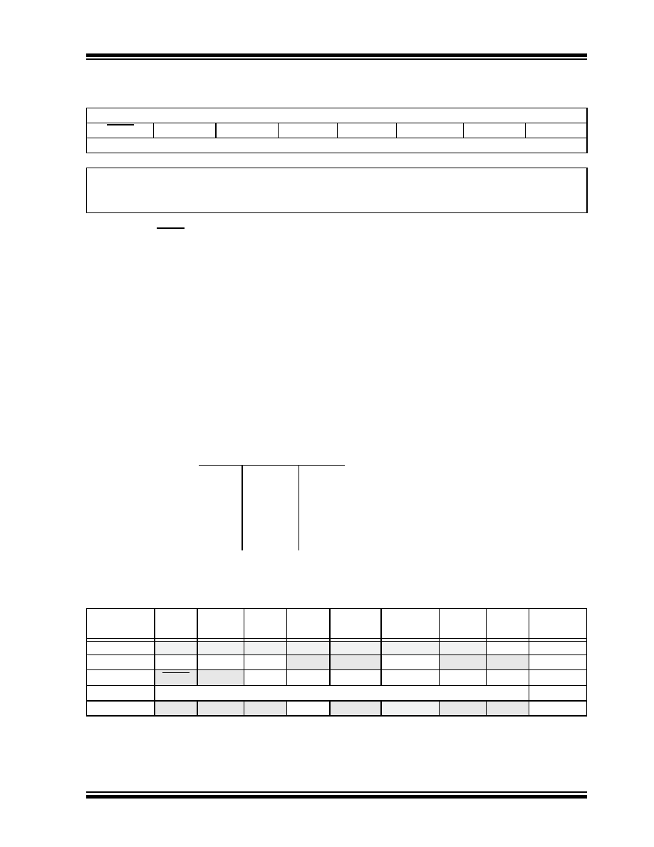
TABLE 11-1:
SUMMARY OF REGISTERS ASSOCIATED WITH TIMER0
REGISTER 11-1:
OPTION_REG: OPTION REGISTER
R/W-1
RBPU
INTEDG
T0CS
T0SE
PSA
PS2
PS1
PS0
bit 7
bit 0
Legend:
R = Readable bit
W = Writable bit
U = Unimplemented bit, read as ‘0’
-n = Value at POR
‘1’ = Bit is set
‘0’ = Bit is cleared
x = Bit is unknown
bit 7
RBPU: PORTB Pull-up Enable bit
1 = PORTB pull-ups are disabled
0 = PORTB pull-ups are enabled by individual PORT latch values
bit 6
INTEDG: Interrupt Edge Select bit
1 = Interrupt on rising edge of INT pin
0 = Interrupt on falling edge of INT pin
bit 5
T0CS: TMR0 Clock Source Select bit
1 = Transition on T0CKI pin or CPSOSC signal
0 = Internal instruction cycle clock (FOSC/4)
bit 4
T0SE: TMR0 Source Edge Select bit
1 = Increment on high-to-low transition on T0CKI pin
0 = Increment on low-to-high transition on T0CKI pin
bit 3
PSA: Prescaler Assignment bit
1 = Prescaler is assigned to the WDT
0 = Prescaler is assigned to the Timer0 module
bit 2-0
PS<2:0>: Prescaler Rate Select bits
000
001
010
011
100
101
110
111
1 : 2
1 : 4
1 : 8
1 : 16
1 : 32
1 : 64
1 : 128
1 : 256
1 : 1
1 : 2
1 : 4
1 : 8
1 : 16
1 : 32
1 : 64
1 : 128
BIT VALUE
TMR0 RATE
WDT RATE
Name
Bit 7
Bit 6
Bit 5
Bit 4
Bit 3
Bit 2
Bit 1
Bit 0
Register on
Page
CPSCON0
CPSON
—
CPSRNG1 CPSRNG0 CPSOUT T0XCS
INTCON
GIE
PEIE
T0IE
INTE
RBIE
T0IF
INTF
RBIF
OPTION_REG
RBPU
INTEDG
T0CS
T0SE
PSA
PS2
PS1
PS0
TMR0
Timer0 Module Register
—
TRISA
TRISA7
TRISA6
TRISA5 TRISA4
TRISA3
TRISA2
TRISA1
TRISA0
Legend: – = Un implemented locations, read as ‘0’, u = unchanged, x = unknown. Shaded cells are not used by the
Timer0 module.
发布紧急采购,3分钟左右您将得到回复。
相关PDF资料
PIC12C508A-04/SN
IC MCU OTP 512X12 8SOIC
PIC12C509A-04/SM
IC MCU OTP 1KX12 8-SOIJ
PIC16LF627T-04I/SO
IC MCU FLASH 1KX14 COMP 18SOIC
PIC12C509A-04/P
IC MCU OTP 1KX12 8DIP
PIC18LC452T-I/PT
IC MCU OTP 16KX16 A/D 44TQFP
PIC12LF1822-I/MF
IC MCU 8BIT FLASH 8DFN
PIC12F1822-I/P
IC MCU 8BIT FLASH 8PDIP
PIC12F1822-I/MF
IC MCU 8BIT FLASH 8DFN
相关代理商/技术参数
PIC16F723AT-I/ML
功能描述:8位微控制器 -MCU 7KB Flash 1.8V-5.5V. 16 MHz int Osc RoHS:否 制造商:Silicon Labs 核心:8051 处理器系列:C8051F39x 数据总线宽度:8 bit 最大时钟频率:50 MHz 程序存储器大小:16 KB 数据 RAM 大小:1 KB 片上 ADC:Yes 工作电源电压:1.8 V to 3.6 V 工作温度范围:- 40 C to + 105 C 封装 / 箱体:QFN-20 安装风格:SMD/SMT
PIC16F723AT-I/MV
功能描述:8位微控制器 -MCU 7KB Flash 1.8V-5.5V. 16 MHz int Osc RoHS:否 制造商:Silicon Labs 核心:8051 处理器系列:C8051F39x 数据总线宽度:8 bit 最大时钟频率:50 MHz 程序存储器大小:16 KB 数据 RAM 大小:1 KB 片上 ADC:Yes 工作电源电压:1.8 V to 3.6 V 工作温度范围:- 40 C to + 105 C 封装 / 箱体:QFN-20 安装风格:SMD/SMT
PIC16F723AT-I/SO
功能描述:8位微控制器 -MCU 7KB Flash 1.8V-5.5V. 16 MHz int Osc RoHS:否 制造商:Silicon Labs 核心:8051 处理器系列:C8051F39x 数据总线宽度:8 bit 最大时钟频率:50 MHz 程序存储器大小:16 KB 数据 RAM 大小:1 KB 片上 ADC:Yes 工作电源电压:1.8 V to 3.6 V 工作温度范围:- 40 C to + 105 C 封装 / 箱体:QFN-20 安装风格:SMD/SMT
PIC16F723AT-I/SS
功能描述:8位微控制器 -MCU 7KB Flash 1.8V-5.5V. 16 MHz int Osc RoHS:否 制造商:Silicon Labs 核心:8051 处理器系列:C8051F39x 数据总线宽度:8 bit 最大时钟频率:50 MHz 程序存储器大小:16 KB 数据 RAM 大小:1 KB 片上 ADC:Yes 工作电源电压:1.8 V to 3.6 V 工作温度范围:- 40 C to + 105 C 封装 / 箱体:QFN-20 安装风格:SMD/SMT
PIC16F723-E/ML
功能描述:8位微控制器 -MCU 7 KB Flash 18V-55V 16 MHz Int Osc RoHS:否 制造商:Silicon Labs 核心:8051 处理器系列:C8051F39x 数据总线宽度:8 bit 最大时钟频率:50 MHz 程序存储器大小:16 KB 数据 RAM 大小:1 KB 片上 ADC:Yes 工作电源电压:1.8 V to 3.6 V 工作温度范围:- 40 C to + 105 C 封装 / 箱体:QFN-20 安装风格:SMD/SMT
PIC16F723-E/MV
功能描述:8位微控制器 -MCU 7KB Flash 1.8V-5.5V RoHS:否 制造商:Silicon Labs 核心:8051 处理器系列:C8051F39x 数据总线宽度:8 bit 最大时钟频率:50 MHz 程序存储器大小:16 KB 数据 RAM 大小:1 KB 片上 ADC:Yes 工作电源电压:1.8 V to 3.6 V 工作温度范围:- 40 C to + 105 C 封装 / 箱体:QFN-20 安装风格:SMD/SMT
PIC16F723-E/SO
功能描述:8位微控制器 -MCU 7 KB Flash 18V-55V 16 MHz Int Osc RoHS:否 制造商:Silicon Labs 核心:8051 处理器系列:C8051F39x 数据总线宽度:8 bit 最大时钟频率:50 MHz 程序存储器大小:16 KB 数据 RAM 大小:1 KB 片上 ADC:Yes 工作电源电压:1.8 V to 3.6 V 工作温度范围:- 40 C to + 105 C 封装 / 箱体:QFN-20 安装风格:SMD/SMT
PIC16F723-E/SP
功能描述:8位微控制器 -MCU 7 KB Flash 18V-55V 16 MHz Int Osc RoHS:否 制造商:Silicon Labs 核心:8051 处理器系列:C8051F39x 数据总线宽度:8 bit 最大时钟频率:50 MHz 程序存储器大小:16 KB 数据 RAM 大小:1 KB 片上 ADC:Yes 工作电源电压:1.8 V to 3.6 V 工作温度范围:- 40 C to + 105 C 封装 / 箱体:QFN-20 安装风格:SMD/SMT